

This post is the fourth of a five part series on microsoldering. If you haven’t yet, you probably want to check out part 1, part 2, and part 3 first.
Microsoldering is high-value repair: You can fix stuff that manufacturers won’t (like water damage and pry damage), which can save you a boatload of money. So I signed up for Jessa Jones’s Practical Board Repair School. But I can’t keep such important knowledge to myself! If you joined me for Day One and Day Two of microsoldering school, you know I learned that schematics are vital for diagnosing problems and a multimeter is invaluable for locating faulty components. On Day Three I learned how to remove, reball, and replace integrated circuits (ICs).
With a good foundation in place, I progressed to the next step. On Day 4 of microsoldering school, I had to split a dual layer iPhone logic board. I won’t lie, this next exercise was like drinking from a firehose. Splitting a PCB sandwich is something we do often here at iFixit, but I’ve never had to put the sandwich back together—and in working order no less!
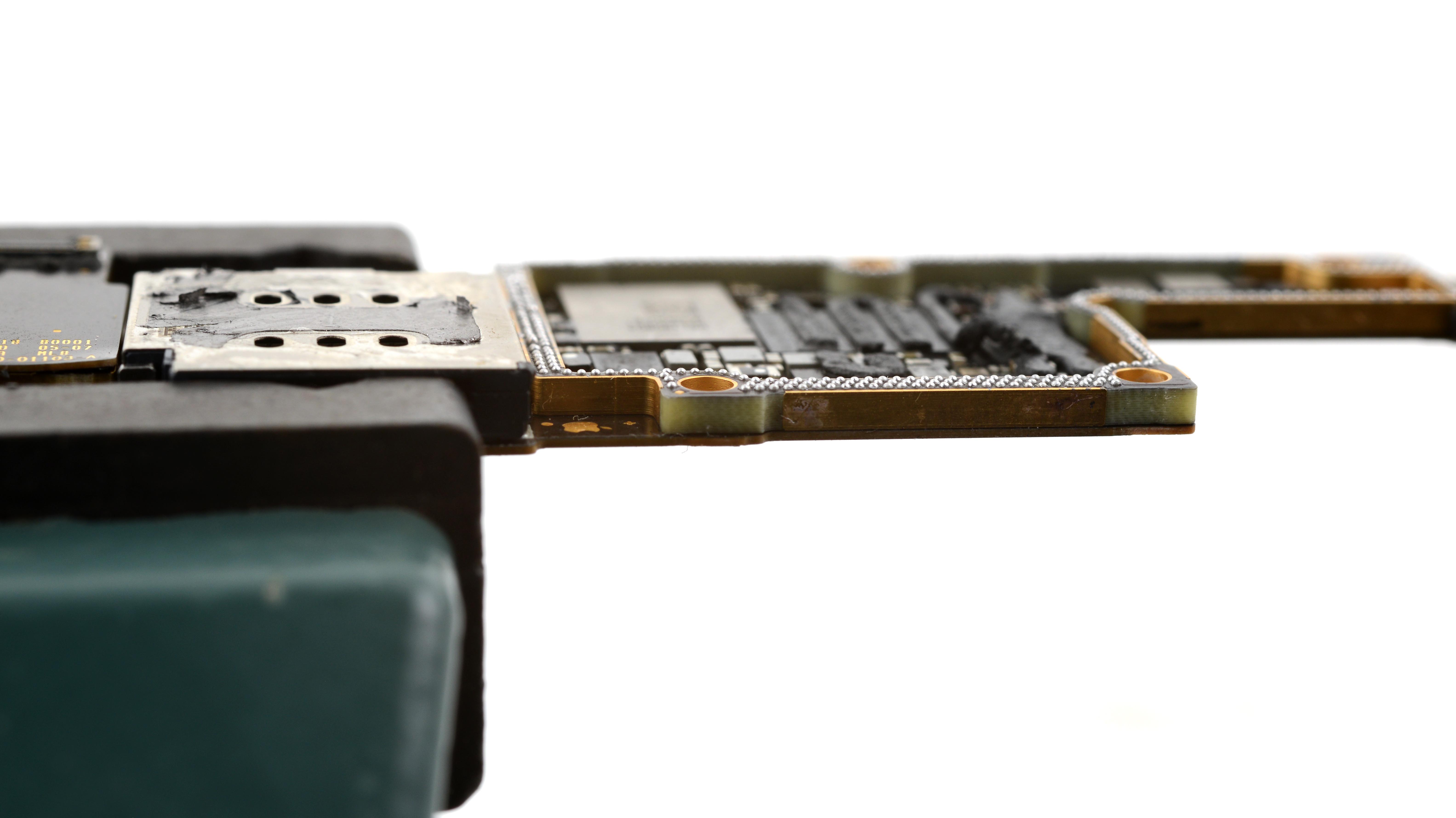
For the uninitiated, modern iPhones have a “sandwiched” logic board consisting of two separate printed circuit boards (PCBs). One PCB houses most of the components relating to processing, storage, security, and power management while the other board mainly handles anything radio and wireless-related (RF) including WiFi, LTE, Bluetooth, 5G, etc. The idea is that you fold the PCB in on itself to reduce the total X and Y area occupied while slightly increasing Z height. Think of it in terms of pizzas and calzones. A sandwiched logic board is a calzone to a standard PCB’s pizza. Your non-Italian friends will tell you they’re pretty much the same thing, the calzone just has the goods on the inside.
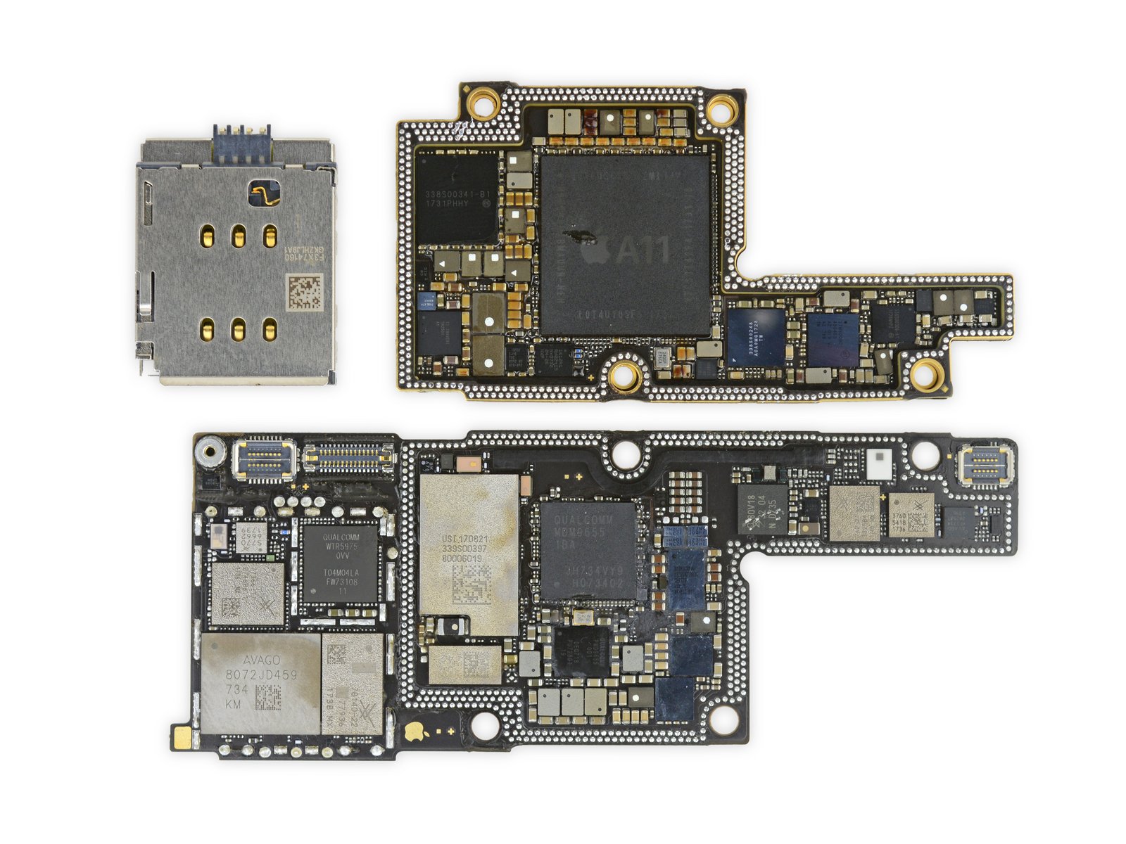
So why would you want to split a logic board? Well aside from performing chip ID for teardowns, these boards will only be split to perform a repair or to recover data. Recovering data is perhaps the harder of the two and in the most extreme cases can involve removing the SoC, NAND, and EEPROM and transplanting all three to a donor board. All three of those components are located inside the PCB sandwich.
In fact, the PCB sandwich houses more than half of the functional components of a modern iPhone’s logic board. As far as repairs go, anything from short circuits caused by blown capacitors to bad cell reception caused by damaged ICs may necessitate splitting a logic board to implement a fix.
The task of splitting a PCB sandwich into its two component parts can be a real doozy but there are some tools that make the process easier and reliably repeatable. One of those tools is a board separator or board splitter. A board splitter is essentially a preheater that is designed around a particular iPhone model. It works by applying controlled heat near the low-melt solder at the seams of one side of the sandwich.
At soldering school, Jessa handed out a board splitter to each of the students for this task. By letting the board splitter do the heavy lifting, the only thing I needed to worry about was carefully lifting the RF layer away from the rest of the PCB.
After separating the PCB sandwich, the next step was to clean up the solder points sitting atop the interposer—that’s the mid-section of the board that connects the bottom layer to the top layer so they can communicate. This part will be easy, I thought. I thought wrong.
After cleaning the old solder away with a copper braid and some flux, I examined the interposer only to find that I had scraped away three of the copper contacts. Jessa proclaimed this blunder an “unscheduled learning opportunity” and proceeded to show us how to fix a ripped copper pad.
Before starting this repair, we looked at which pads were missing. With the assistance of schematics, Jessa taught as another invaluable lesson: don’t bother fixing the things that don’t need to be fixed. You see, some of these pads were ground pads. And yes, ground pads do perform a function but in this instance, they’re mostly acting as redundancies. Since a system’s ground plane is connected throughout, we generally don’t need to worry about fixing a contact to ground if others already exist. On this interposer, we have lots of other contacts going to ground. The result is that of the three missing pads, only one needed to be fixed!
Jessa readied a replacement copper pad. But she had to do some prep work before she could put it on the board.
With the pad gone, the only trace of copper was a tiny wire receding into the PCB that must have been less than the width of a human hair. That tiny spot is what Jessa tinned with solder and then soldered a lug on to, something she’s done many times before.
But that wasn’t the end of this repair. The solder from the tiny copper wire to the lug was merely to establish an electrical connection to the pad, not to hold the pad in place. For that task Jessa used “The Green Stuff,” a compound which I can only assume is comprised of the distilled tears of failed students past and the trapped souls of anti-repair lobbyists. Only then did she apply the replacement pad.
With the mixture expertly deposited around the edges of the replacement pad, she threw a UV light over the area for a few seconds and the repair was complete. The resin solidified partly on the lug and mostly on the board, securing the lug in place. I cannot imagine how much practice must have gone into performing this type of repair but she definitely made it look deceptively easy. It was an impressive display of workmanship and the kind of fine motor skills you’d expect from a neurosurgeon.
Fixing traces and pads using solder lugs definitely grabbed my interest—it’s a fascinating repair. From the advanced repair task of splitting a logic board to the advanced repair task of fixing a ripped copper pad the width of the tip of a ballpoint pen, I was racking up advanced repair merit badges. But I was still a bit overwhelmed. It was clear to me that I was going to need a lot of practice to truly be effective at any of these repairs. Fixing a ripped pad is certainly a useful skill to have but do yourself a favor, avoid this problem altogether. Don’t scrape the pads with a copper braid when cleaning solder!
With the pads repaired, it was time to reball the interposer and prepare the RF board for reassembly. The board splitter we used doubled as a reballing platform and, with the correct stencil, we simply had to implement the reballing techniques we learned on Day 3. Reballing the interposer is definitely a trickier task than reballing an IC that only has a dozen or so solder points, but as with everything else, it’s just a matter of getting enough practice in. It’s frustrating to mess up the solder points but at least it’s a mistake that can be cleaned up and attempted again.
With the interposer prepped, the only thing left to do is to place the RF board over the interposer and apply enough heat to melt those solder balls. With any luck—or lots of skill if you’re a pro!—the solder balls are lined up and evenly spaced and they should just adhere to the copper pads on the RF board.
Of course there’s only one way to know if you’re done with the repair and that’s to test the board! If it boots up then you’re done! If not, it’s time to get more practice in. That’s the beauty of this repair. If you’re careful and patient (i.e., you don’t rip up pads left right and center like I did), you can attempt this repair over and over until you get it right. Practice makes perfect!
Day four was intense, but Jessa told us we had all the core microsoldering skills in place by the end of it—good thing, too, because there was just one day left. In our final day of soldering school, I took what I learned from the previous four days and applied it to a personal project. This is where the real value of learning microsoldering comes into focus, as that broken device that’s been sitting around the workshop for months finally gets a new lease on life! Stay tuned.


0 Comments